NVIDIA Harnesses Vera CPU to Speed Up Design of Next-Generation CPUs and GPUs
The complexity of modern chip design continues to grow as engineering teams work to develop increasingly sophisticated CPUs, GPUs and AI systems. To help meet that challenge, NVIDIA is collaborating with industry leaders Cadence and Synopsys to optimize critical electronic design automation (EDA) applications for the NVIDIA Vera CPU. NVIDIA is now deploying Vera across [...]
Key Takeaways
- NVIDIA is now deploying Vera across EDA workflows used to develop its next generation of CPUs and GPUs, demonstrating how high-performance CPU architecture can help accelerate some of the industry's most demanding engineering workloads.
Accelerating Critical EDA Workloads What's at stake is the pace of chip production.
- While GPUs and AI have accelerated many aspects of chip design, several critical EDA workloads remain heavily dependent on CPU performance.
Logic simulation, formal verification and portions of digital implementation often depend on fast individual cores, efficient memory systems and strong overall throughput.
- Early testing on selected production-class workflows shows promising results.
Cadence Jasper , a formal verification platform, uses smart proof technology and machine learning to find and fix bugs and improve verification productivity early in the design cycle.
- Bringing Vera to the Design Process NVIDIA is deploying Vera throughout the EDA workflows used to create future NVIDIA processors.
- Multiple verification and implementation technologies then work together to transform that design into manufacturable silicon.
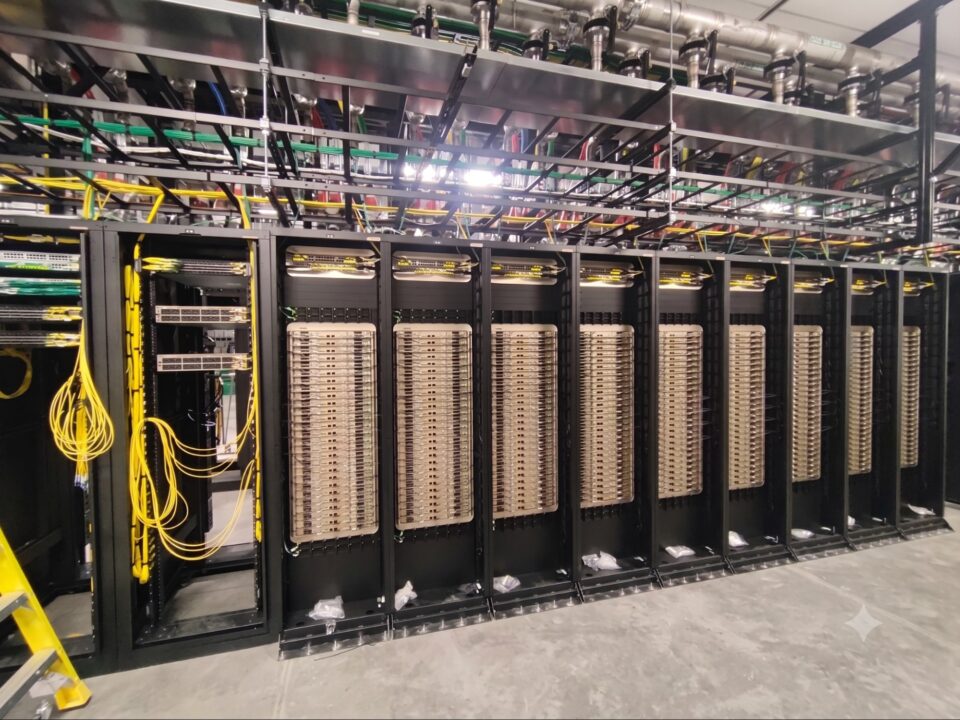
The complexity of modern chip design continues to grow as engineering teams work to develop increasingly sophisticated CPUs, GPUs and AI systems. To help meet that challenge, NVIDIA is collaborating with industry leaders Cadence and Synopsys to optimize critical electronic design automation (EDA) applications for the NVIDIA Vera CPU. NVIDIA is now deploying Vera across EDA workflows used to develop its next generation of CPUs and GPUs, demonstrating how high-performance CPU architecture can help accelerate some of the industry's most demanding engineering workloads.
Accelerating Critical EDA Workloads What's at stake is the pace of chip production. In turn, the tempo of industry technologies that stand to benefit from boosted EDA workloads, driving development momentum. Simulation, verification and implementation technologies play a central role in semiconductor development.
Long before a chip reaches manufacturing, engineers spend years validating behavior, identifying corner cases and refining designs through thousands of iterations. While GPUs and AI have accelerated many aspects of chip design, several critical EDA workloads remain heavily dependent on CPU performance. Logic simulation, formal verification and portions of digital implementation often depend on fast individual cores, efficient memory systems and strong overall throughput.
That makes CPU architecture an important factor in determining how quickly engineering teams can validate designs, explore alternatives and move products toward tapeout. Highlighting Early Results With Cadence and Synopsys NVIDIA's initial testing includes several leading EDA applications. The results highlight Vera's ability to accelerate two of the most compute-intensive stages of modern chip design.
Early testing on selected production-class workflows shows promising results. Cadence Jasper , a formal verification platform, uses smart proof technology and machine learning to find and fix bugs and improve verification productivity early in the design cycle. Synopsys VCS, a high-performance functional verification solution used to simulate and validate complex chip designs before fabrication, used the same number of cores in the test.
Both applications showed up to 1.5x higher performance on selected workloads. Beyond benchmark results, NVIDIA is working closely with both companies on application profiling, software optimization and system-level tuning designed to improve engineering productivity across a broader range of workflows over time. Bringing Vera to the Design Process NVIDIA is deploying Vera throughout the EDA workflows used to create future NVIDIA processors.
Vera combines 88 custom NVIDIA Olympus CPU cores with a high-efficiency LPDDR5X memory subsystem and second generation NVIDIA Scalable Coherent Fabric designed to deliver strong per-core performance, high memory bandwidth and consistent low latency for demanding engineering applications. These capabilities are particularly important for workloads that mix latency-sensitive jobs with large-scale regression testing across compute farms. Faster execution can shorten individual verification runs, while greater throughput enables engineers to evaluate more design alternatives and complete more validation within the same development window.
Going From RTL to Silicon After defining a processor's architecture and microarchitecture, engineers describe much of its behavior at the register-transfer level (RTL). Multiple verification and implementation technologies then work together to transform that design into manufacturable silicon.
For more details please read the original article at NVIDIA Blog.
Continue Learning
Comments
Comments appear only after moderation. Your email identifies your submission to the moderator and is never displayed here.
No approved comments yet.